Bilkent researchers lead by Dr. Onur Tokel of the Department of Physics and Dr. Ömer İlday of the Department of Electrical and Electronics Engineering and Physics have for the first time demonstrated truly 3D fabrication inside silicon wafers, opening the way to 3D electronic and photonic devices. The team described their work in the latest issue of Nature Photonics, a top ranked journal.
This new method uses a laser beam to create 1 µm-sized building blocks (one-hundredth of the diameter of the human hair) in a sliver of silicon, which are then used to fabricate new types of silicon devices.
Silicon is the bedrock of modern computers, mobile communications and photonic devices. These technologies are continually enabling more functionality and speed. Precisely because of such amazing successes, it may be surprising to learn that virtually none of these advances are taking advantage of the vast space available below the surface, inside the silicon wafers. Thus, when the team decided to make use of the unused volume inside silicon, there was no method that could enable their goal. However, they soon found that a focused laser can help to overcome the “dimensional barrier,” enabling the assemblage of 3D elements for advanced functionality inside silicon.
“We achieve this by exploiting dynamics arising from nonlinear laser interactions, leading to controllable building blocks,” says Prof. Onur Tokel of the Department of Physics at Bilkent, who is the lead author of the paper. “In any 3D fabrication method, there is a trade-off between speed, resolution and complexity. With our approach, we’re hitting the sweet spot. The key is recognizing that most practical components can be made out of rod- or needle-like building blocks. Our method enables the creation of such blocks, while also preserving a width of about one micrometer. Better yet, these blocks can be combined to create a 2D layer, or even more complex 3D shapes, simply by scanning the laser beam over the chip.”
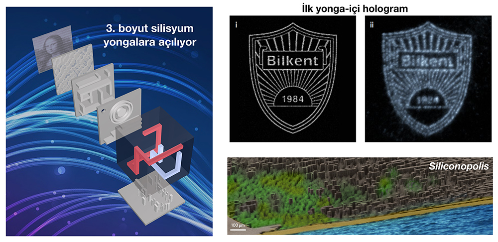 Following this achievement, the researchers demonstrated various 3D optical elements directly inside silicon, such as lenses, waveguides and holograms. Inspired by the successes of “on-chip” devices on various materials, they introduced the term “in-chip” as a shorthand descriptor for this new class of devices.
A further outcome is related to 3D printing or sculpting. The researchers found that by exposing the laser-modified areas to a chemical etchant, 3D sculpting of the entire wafer is possible. “I should note that this is a direct laser-writing approach, without the use of masks – inexpensive compared to alternative methods,” notes Dr. Serim İlday, also of the Department of Physics at Bilkent and one of the coauthors of the paper.
“The possibilities are endless. It’s likely that the method will enable entirely new in-chip devices, such as Si-photonics components, or meandering microfluidic channels that could be used to efficiently cool electronic chips,” observed Prof. Ömer İlday, another coauthor of the paper and member of the Electrical and Electronics Engineering and Physics departments. “As a matter of fact,” he continued, referring to follow-up studies the team is working on, “we have already started to develop new in-chip architectures and functionalities, such as waveguides and laser slicing of wafers.”