A groundbreaking study published in “Nature Communications” unveils a method for laser nanofabrication directly within silicon, with significant implications for the fields of nanophotonics, silicon photonics and 3D electronic-photonic integrated systems.
 The research, led by Asst. Prof. Onur Tokel from the Department of Physics and UNAM – National Nanotechnology Research Center showcases the ability to create the first controlled nanostructures deep inside silicon wafers, achieving feature sizes as small as 100 nm, marking a significant leap from the current state-of-the-art.
“Our approach is based on localizing the laser energy within a semiconductor material to an extremely small volume, such that one can exploit emergent field enhancement effects analogous to those in plasmonics. This leads to sub-wavelength and multi-dimensional control directly inside the material,” explained Dr. Tokel.
“That the researchers were able to achieve nano-scale features is spectacular,” says Maxime Chambonneau, a researcher at the University of Jena, in Germany, who was not involved in the work. “Our findings introduce a new nano-fabrication paradigm,” explains Dr. Tokel. “The ability to fabricate at the nano-scale directly inside silicon opens up a new regime toward further integration and advanced photonics. We can now start asking whether complete three-dimensional nano-fabrication in silicon is possible. Our study is the first step in that direction.”
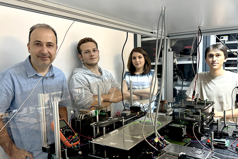
The research team consists of Rana Asgari Sabet, Aqiq Ishraq, Alperen Saltik, Mehmet Bütün and Onur Tokel from the Department of Physics and UNAM at Bilkent University. The manuscript and funding information can be reached at Nature Commun. 15, 5786, 2024. Relevant material can be reached at the IEEE Spectrum magazine, September print issue.
For More Information: https://www.nature.com/articles/s41467-024-49303-z